top of page
Galvo Mirror Scanning uses ultra-responsive galvanometric mirrors to rapidly steer the laser beam across a sample. Unlike traditional mechanical stage scanning—which involves moving the sample itself—this technique redirects the beam in microseconds, allowing for non-contact, vibration-free scanning with sub-micron precision.
Galvo Mirror Scanning uses ultra-responsive galvanometric mirrors to rapidly steer the laser beam across a sample. Unlike traditional mechanical stage scanning—which involves moving the sample itself—this technique redirects the beam in microseconds, allowing for non-contact, vibration-free scanning with sub-micron precision.
Galvo Mirror Scanning uses ultra-responsive galvanometric mirrors to rapidly steer the laser beam across a sample. Unlike traditional mechanical stage scanning—which involves moving the sample itself—this technique redirects the beam in microseconds, allowing for non-contact, vibration-free scanning with sub-micron precision.
Galvo Mirror Scanning uses ultra-responsive galvanometric mirrors to rapidly steer the laser beam across a sample. Unlike traditional mechanical stage scanning—which involves moving the sample itself—this technique redirects the beam in microseconds, allowing for non-contact, vibration-free scanning with sub-micron precision.
HOME > TECHNOLOGIES
Confocal Laser Scanning

Technology Overview
Galvo Mirror Scanning uses ultra-responsive galvanometric mirrors to rapidly steer the laser beam across a sample. Unlike traditional mechanical stage scanning—which involves moving the sample itself—this technique redirects the
beam in microseconds, allowing for non-contact, vibration-free scanning with sub-micron precision.
Specifications
.png)
.png)
Key Advantages of Nanobase Galvo Mirror Technology
.png)
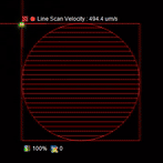
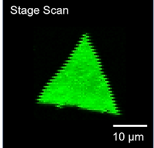
Mapping Performance Comparison (Galvo Scan VS Stage Scan)
.png)
.png)
• Laser wavelength: 532 nm
• Objective: 40X (N.A 0.75)
• Laser Spot Diameter: 0.9 μm
• Mapping Range: 50 x 50 μm
• Step Distance: 0.5 μm
Galvo Mirror Scanning Technology
Galvo Mirror Scanning is a core technology in advanced Raman mapping, enabling ultra-fast, precise, and localized measurements. In the NANOBASE SMART™ Mapping Platform, this technology is integrated with motorized stage movement to form a hybrid system—combining the high-speed agility of galvo scanning with the wide-area coverage of stage mapping. The result is unmatched speed, flexibility, and precision in one platform.
.png)
Technology Overview
At Nanobase, we’ve redefined how Raman signals are captured with our proprietary Slit-Binning technology—a powerful enhancement to signal processing that dramatically improves sensitivity and data quality without compromising resolution. Traditional CCD binning methods often sacrifice signal integrity or spatial resolution. Our Slit-Binning approach intelligently integrates only the effective slit area on the detector, eliminating background noise and optimizing the signal-to-noise ratio (SNR). This leads to sharper, clearer spectra, even from extremely weak Raman signals.
.png)
Z-Axis Profiling Capability
Our Slit-Binning confocal design not only simplifies maintenance compared to traditional pinhole confocal systems but also enables precise Z-axis profiling, allowing detailed depth analysis and layer-by-layer measurements with high repeatability. This combination of optical, mechanical, and design innovations ensures consistently dependable Raman performance.
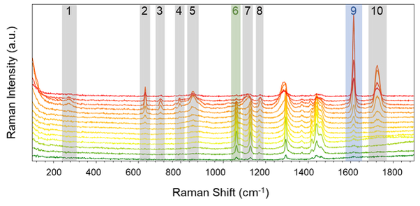
Application Example: Multiplayer Film Analysis (PET/PE/EVOH/PE)
.png)
.png)
Z-step size: 0.3 μm / Exposure time: 1 sec / Depth range: 0–60 μm
Peak at ~1061 cm⁻¹ for EVOH and ~1617 cm⁻¹ for PET clearly separated by depth.

Live-Focus
Technology Overview
Live-Focus is Nanobase’s real-time laser auto-focusing function, powered by its proprietary Laser Auto-Focus Module. This intelligent system continuously tracks and automatically adjusts the laser’s focal point during measurement (including scanning), ensuring optimal focus even on tilted, uneven, or structured surfaces.(including scanning), ensuring optimal focus even on tilted, uneven, or structured surfaces.

1x speed
.png)
Specifications
.png)
•The performance may be limited by the laser power used in the measurement.
•The performance may be limited in samples with low surface reflectivity or rough surfaces causing diffuse reflection.
Live-Focus Mapping Performance
.png)
Depth of Field
In Raman spectroscopy, the Depth of Field (DOF) is the range where the laser stays sharply focused, ensuring precise signal acquisition. Accurate focus improves signal strength, reduces noise, and depends on factors like laser wavelength, objective lens, and numerical aperture.
.png)
.png)

SMART Mapping
Technology Overview
Nanobase Raman systems offer three distinct scan modes, each optimized for specific analytical needs and spatial resolutions. From rapid surface inspection to high-resolution mapping, these modes empower researchers to adapt their measurement strategy without compromising data quality.
Hybrid Architecture: Galvo Mirror + Motorized Stage
.png)
At the core of our system is a hybrid scanning mechanism that combines a galvo for fast beam steering with a motorized stage for precise movement.
The Galvo Mirror enables rapid spot switching and high-speed scanning, while the Motorized Stage provides accurate positioning and large-area mapping.
Together with built-in autofocus, this dual approach ensures sharp focus and clear imaging across the full measurement range.
Scan Mode Comparison
.png)
.png)
NANOBASE SMART™ Mapping
.png)
.png)
Adaptable to Any Sample Size or Resolution
From sub-micron spatial resolution for microstructures to large-area samples, Nanobase systems adapt seamlessly to a wide range of research scenarios. Whether you're performing quick evaluations or conducting in-depth surface analyses, you can fine-tune your scanning strategy to meet your analytical goals.

SpectraBoost
Technology Overview
At Nanobase, we believe that true performance in Raman spectroscopy begins with the right detector — not a one-size-fits-all solution. Unlike conventional systems that rely on a single detector to cover a broad wavelength range, Nanobase takes a different approach: we provide Raman products equipped with high-performance CCD detectors, each optimized to deliver the best performance for its specific laser wavelength.
This wavelength-specific optimization allows us to achieve:
• Maximum sensitivity at the target Raman shift range
• Minimized background noise, even at low light levels
• Fast mapping enabled by strong signal output
• Reliable performance across diverse Raman applications
.png)
Raman Signal
High QE CCD
High signal intensity
Low QE CCD
Low signal intensity
Specifications Summary of the Detector
• Active pixels: 1931 × 1451 pixels
• Pixel size: 4.54 × 4.54 μm
• Dark current: ~0.0002 e-/pixel/sec
• High detector sensitivity peak QE of 74%
• Wavelength range: 400 ~ 800 nm ( > QE 40%)
.png)
.png)
Specifications Summary of the Detector
• Back-illuminated CCD, Deep-Depletion with anti-fringing
• Active pixels: 2000 × 256 pixels
• Pixel size: 15 × 15 μm
• Dark current: As low as 0.033 e-/pixel/sec
• High detector sensitivity peak QE of 94%
• Wavelength range: 400 ~ 950 nm ( > QE 40%)

Specifications Summary of the Detector
• Active pixels: 1024 pixels
• TE cooling down to -90 °C
• Pixel size: 25 × 500 μm
• Dark current: As low as 12.0 ke-/pixel/sec
• High detector sensitivity peak QE of 85%
• Wavelength range: 1.0 ~ 1.6 µm ( > QE 80%)
.png)
.png)
This strategic hardware configuration gives Nanobase a clear edge over competitors using generic detectors, ensuring our systems are not only more sensitive, but also more accurate and application-ready from the start.
.png)
Technology Overview
At the heart of Nanobase’s Raman spectrometers lies a Transmission Volume Phase Holographic (VPH) Grating—a key optical component that enables exceptional sensitivity with minimal noise. Unlike conventional reflective gratings, a transmission VPH grating disperses light by passing it through a holographically recorded volume phase structure. This unique design offers several advantages:
• High Diffraction Efficiency: Maximizes signal throughput, ensuring that even the faintest Raman signals are preserved.
• Low Stray Light: Reduces unwanted background light, improving spectral contrast and signal-to-noise ratio (SNR).
• Minimal Ghosting: Provides cleaner spectra without the artifacts that often accompany reflective grating designs.
• Compact Optical Path: Allows for more stable alignment and reduced optical aberration
.png)
Optimized Transmission Grating for Peak Efficiency
.png)
Our Raman spectrometers feature a custom manufactured transmission grating engineered to deliver maximum diffraction efficiency at the target spectral wavelength.
Interchangeable-Grating Spectrometer
Our spectrometers are also designed to allow easy replacement of the grating with different groove densities (lpmm). This flexibility lets users optimize spectral resolution and wavelength range for specific applications—whether prioritizing fine detail or broader coverage.
Easy Grating Replacement
.png)
bottom of page